Reading time
4 Minutes
Published
GaN and SiC Semiconductors- Driving the Next Generation of Power Electronics
Management Summary
GaN & SiC Semiconductors– High Power and Efficiency Beyond Silicon
Get a concise overview – the detailed technical insights and analyses follow in the main article.
Thanks to their very high electron mobility, GaN FETs allow lateral device structures, reducing intrinsic capacitances and eliminating recovery losses. They are optimised for high-power and high-frequency applications.
SiC FETs provide higher thermal conductivity than silicon and benefit from a mature manufacturing process for high-voltage applications. They are designed for high-power, high-voltage systems.
Key advantages of GaN and SiC over silicon:
- Higher output power
- Improved efficiency
- Reduced cooling requirements
- More compact designs
- Higher reliability under extreme conditions
Challenges:
-
Limited second-source availability
-
Higher component costs (minimal in some performance ranges; simplified architectures possible)
-
GaN-specific considerations:
-
Limited availability of driver circuits and DCDC controllers
-
Fewer solutions for low-voltage applications
-
Increased demands on driver circuits and PCB layout
-
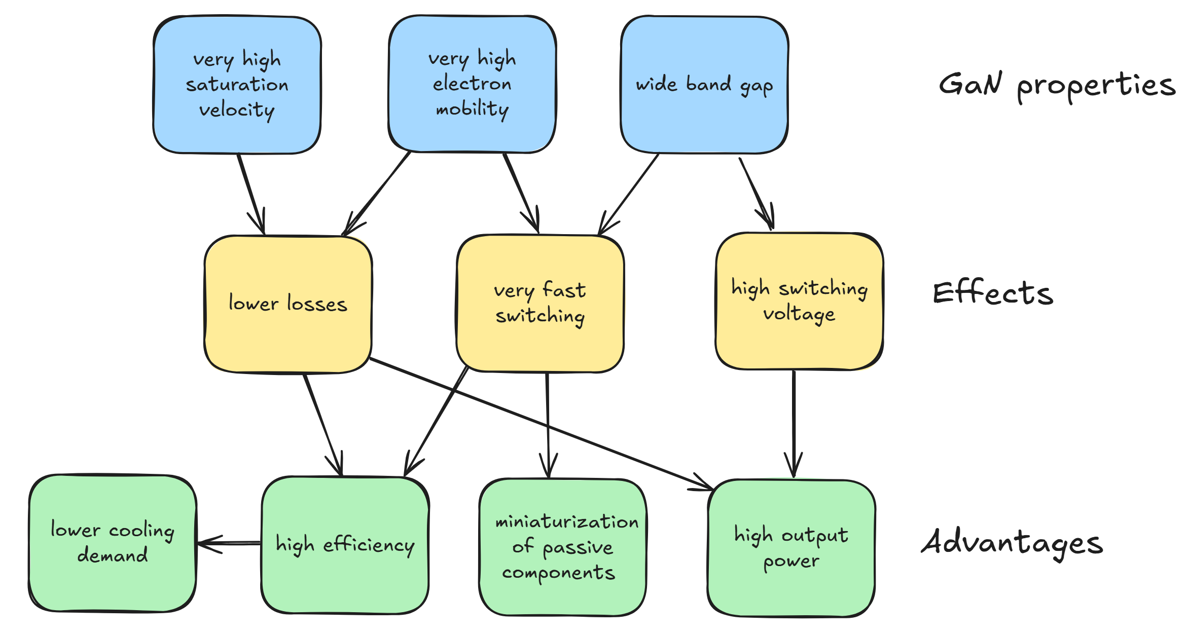
Effects and Advantages of GaN
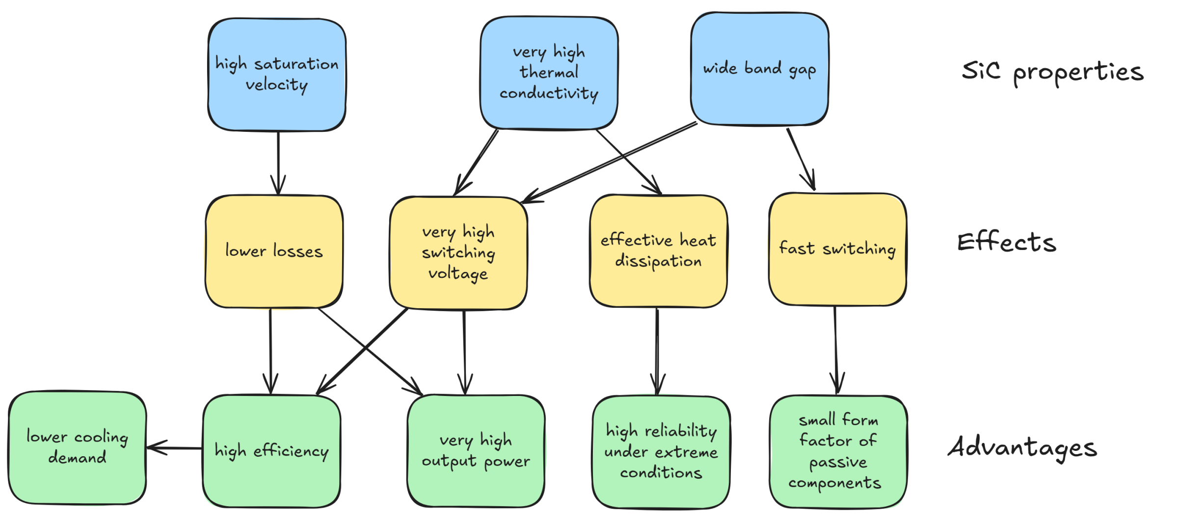
Effects & Advantages of SiC
Insight in brief
Wide band-gap materials such as GaN (Gallium Nitride) and SiC (Silicon Carbide) offer significant advantages in material properties compared to Si (Silicon). GaN FETs are optimized for power and high-frequency applications. SiC FETs are mainly used in power and high-voltage applications.
Article topics:
- Technical characteristics of wide band-gap materials
- Lateral architecture of GaN FETs
- Hands-On Test: GaN vs Silicon
- Market trends
Introduction
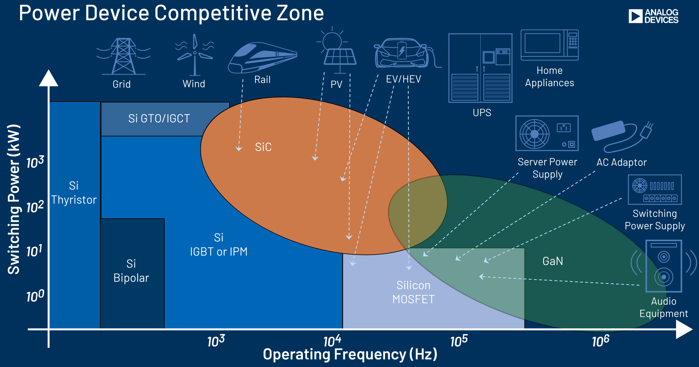
Decarbonization policies, together with growing societal pressure, are driving industries to invest heavily in more efficient energy conversion and accelerated electrification. This trend has significantly boosted the development of GaN (Gallium Nitride) and SiC (Silicon Carbide) technologies in recent years. Wide band-gap (WBG) semiconductors - such as GaN and SiC - enable performance and efficiency levels that conventional Silicon (Si) devices can no longer achieve.
Definition of Wide Band-Gap (WBG) Material
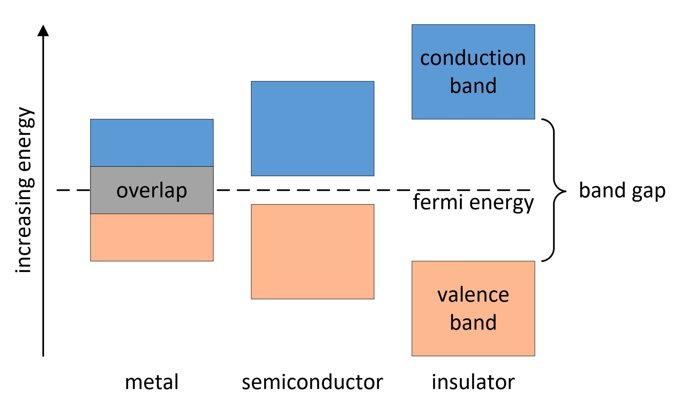
The band gap is the energy an electron needs to move from the valence band to the conduction band. If this gap is large (greater than 2 eV), the material is called a wide band-gap material.
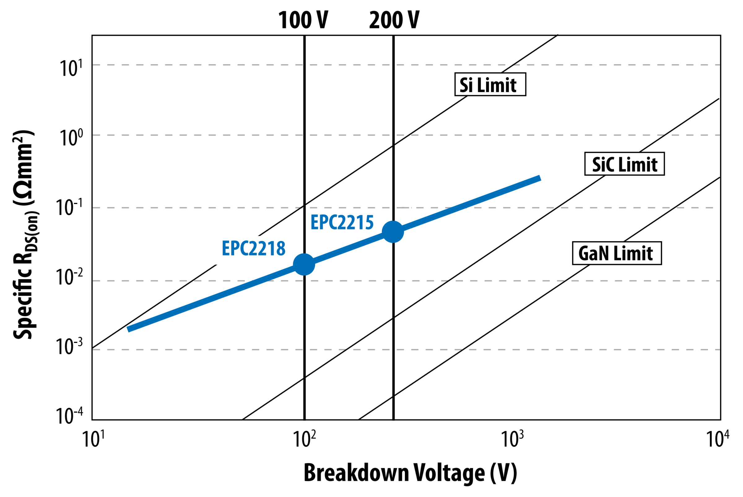
Silicon has a band gap of 1.1 eV. Modern wide band-gap materials have two to three times that value. GaN (3.4 eV) and SiC (3.2 eV) are among the most important materials for electronics.
A large band gap means:
- Higher voltage resistance
→ A larger band gap lets a material handle stronger electric fields before it breaks down - Lower leakage currents
→ WBG materials stay stable at high temperatures and don’t leak current - Faster switching
→ Especially GaN can change its conduction state extremely quickly - perfect for high-frequency applications
Comparison of the properties of GaN, SiC and Si
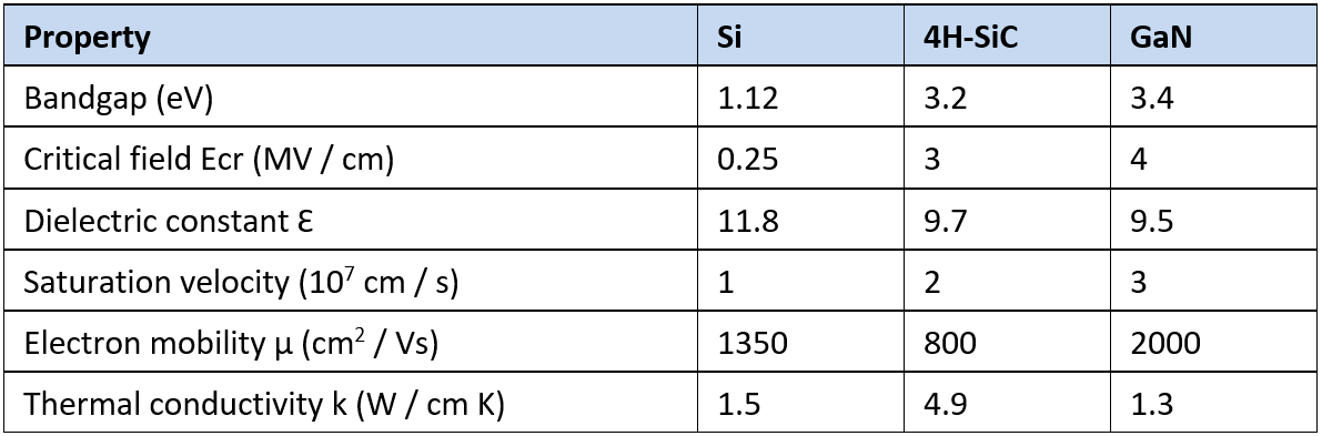
...Compared to Si, SiC and GaN can withstand stronger electric fields and therefore tolerate higher voltages before breakdown...
GaN has higher electron mobility and saturation velocity compared to SiC and Si.
Electron mobility describes how quickly electrons can move through the semiconductor. A high electron mobility transistor (HEMT) allows faster switching and reduces switching losses. High electron mobility also helps lower RDS(on), along with other design factors.
Saturation velocity is the point at which increasing the electric field no longer speeds up electron movement.
In GaN devices, the gate electrode takes up very little chip area, which keeps parasitic capacitance very low. Thanks to these properties, GaN semiconductors enable very high switching frequencies.
"GaN is a semiconductor material with excellent properties for power and high-frequency applications."
SiC has much higher thermal conductivity compared to GaN and silicon, making it better suited for high-voltage applications such as electric vehicles, data centers, solar power, and rail systems. These applications do not necessarily require very high switching frequencies but depend on high switching voltages.
SiC FETs have been available on the market for a longer time and feature a more mature manufacturing technology for high-voltage applications.
"SiC is a semiconductor material with excellent properties for power and high-voltage applications."
GaN semiconductor structure
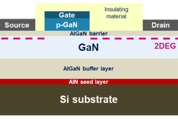
Lateral Structure of GaN FETs
Unlike Si and SiC FETs, most GaN FETs have a lateral structure, meaning the source, drain, and gate are all on the same surface level.
GaN’s high electron mobility, high saturation velocity, and high breakdown field strength enable a very compact lateral design. This structure results in a small gate area, short current loops, and reduced parasitic effects (R/L/C), which improve EMC performance and switching speed.
Due to its lateral structure, a GaN FET has no traditional body diode and therefore no reverse-recovery current. This significantly reduces recovery losses during fast switching, especially in half-bridge operation.
Design Challenges
On the downside, the compact structure also has challenges. Compared to Si FETs, GaN FET gates are much more sensitive to disturbances, gate ringing/bouncing, and high dV/dt applications. The maximum VGS is often limited to about ±6 V, and the VGS(th) typically ranges from 1 V to 2 V.
The dead time (the period when both FETs in a half-bridge are off) must be minimized to avoid high reverse conduction losses. During dead time, current flows in the opposite direction through the two-dimensional electron gas layer (2DEG) of the lower FET. This is possible because of the symmetric source/drain structure relative to the gate, once the condition VGD = VGS + VSD > VGS(th) is met. In this stage, VSD is higher than the forward voltage of a body diode, so the power loss is greater than in a Si FET.
Very fast switching is possible thanks to the low parasitic capacitances (CGS and CGD) of GaN FETs. However, dead time cannot be reduced to zero, as this could cause a FET shoot-through. The challenge is to identify the optimal dead time in the circuit.
Driver and PCB Requirements
The requirements for the FET driver and PCB layout are significantly higher due to the described effects compared to designs using Si or SiC FETs. Special attention must be paid to minimizing gate and power loop lengths, as parasitic inductances have a greater impact during fast switching events and can lead to increased losses.
Substrate Technology and Market Adoption
Another key element in the design is the substrate material used for the epitaxial growth of the GaN layer. The technology evolved from GaN-on-Sapphire (used for LEDs) to GaN-on-GaN (expensive and difficult to manufacture), then to GaN-on-SiC (for RF and radar applications), and finally to GaN-on-Si. GaN-on-Si ultimately became the breakthrough for mass-market GaN electronics, as it combines the high performance of GaN with the cost-efficient manufacturing of silicon.
GaN-on-Si technology reached maturity between 2013 and 2017, with a commercial breakthrough around 2018 when it began to be adopted in chargers, power supplies, and electric vehicles.
Hands-On test: GaN vs Si
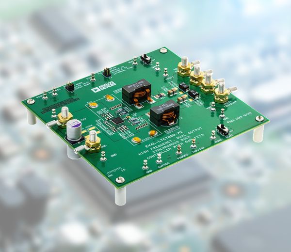
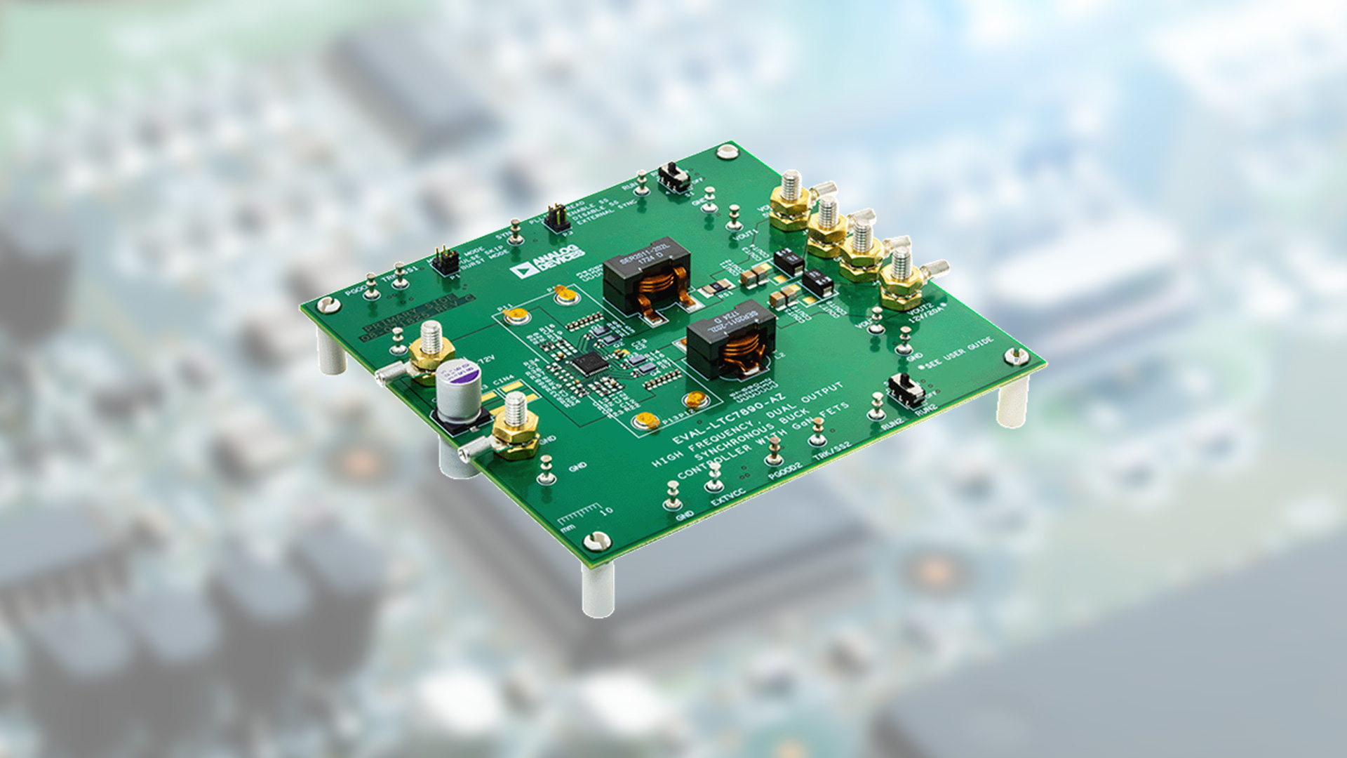
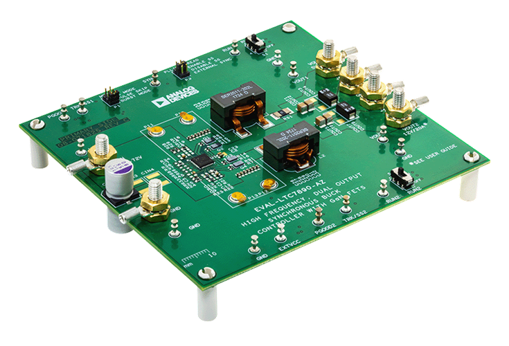
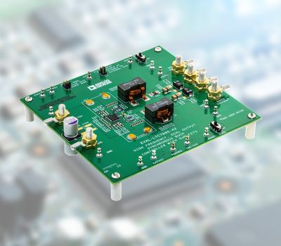
For the performance comparison, the two evaluation kits EVAL-LTC7890-AZ und EVAL-LTC7890-BZ from Analog Devices were used.
Operating Condition
GaN FETs: EPC 2218
VIN: 48 V | OUT1: 5V, 10 A | OUT2: 12 V, 10 A | fsw: 500kHz
Operating Condition
Si FETs: Infineon BSC146N10LS5 und BSC070N10LS5
VIN: 48 V | OUT1: 5V, 10 A | OUT2: 12 V, 10 A | fsw: 500kHz
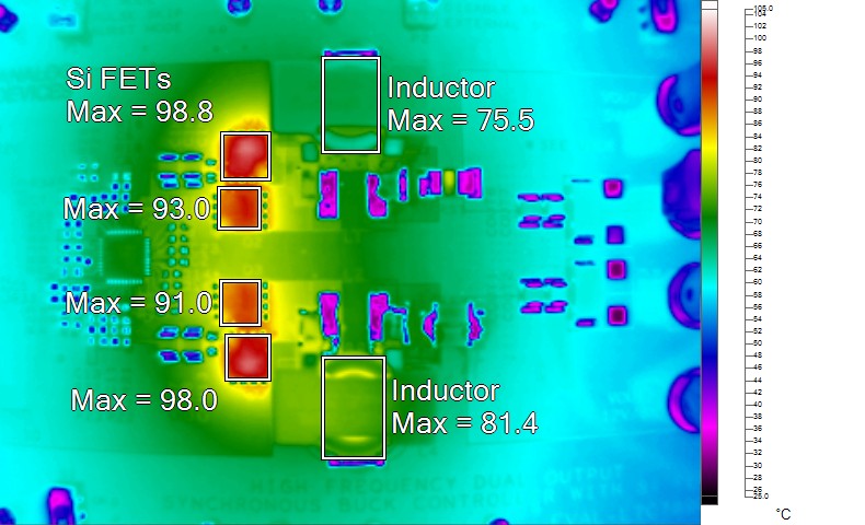
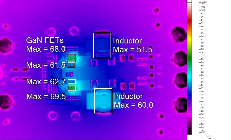
By using GaN FETs, power losses can be significantly reduced, and there is again flexibility in terms of output current, input voltage, or form factor. Testing confirmed that when using GaN FETs, the following parameters can be adjusted to achieve approximately the same thermal stress as with Si FETs:
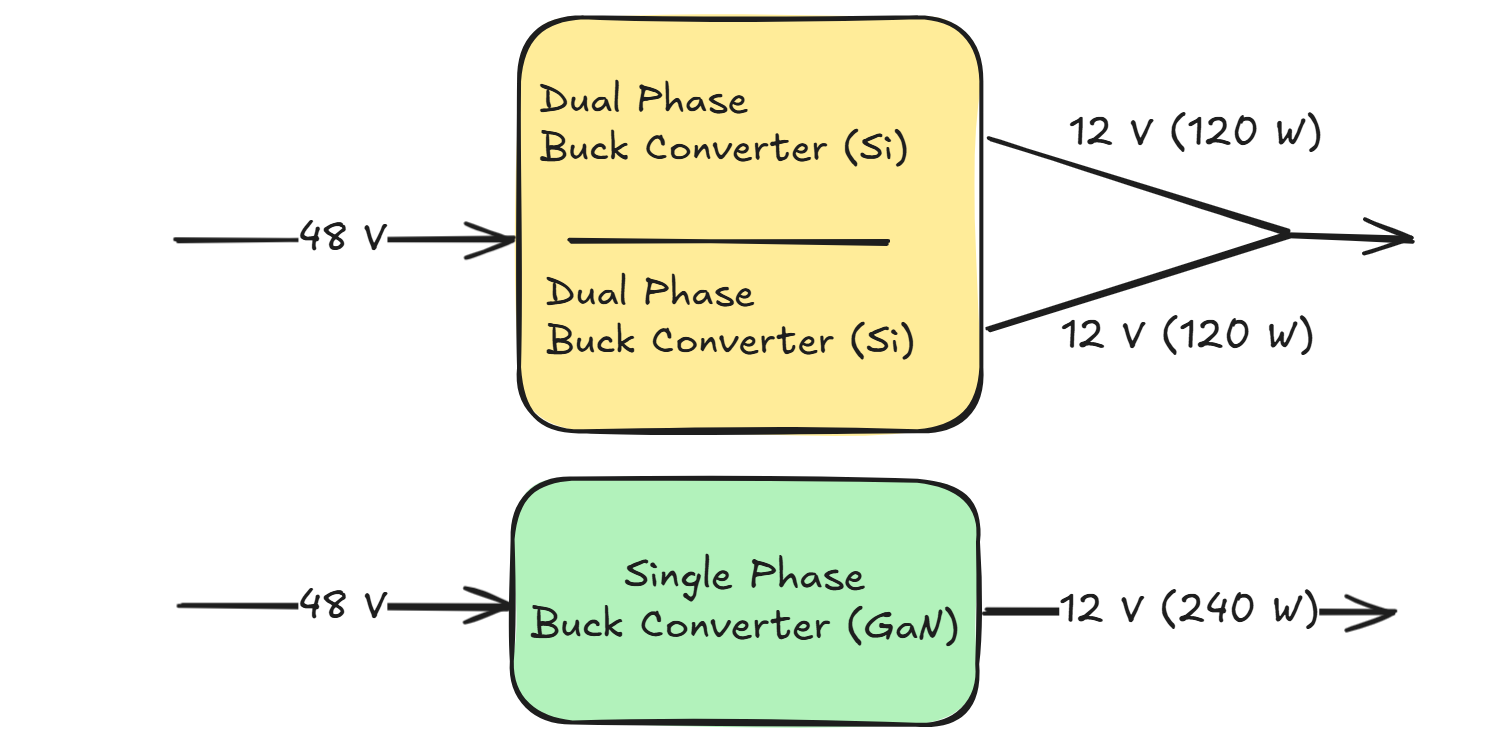
- The output current can be increased by a factor of 1.5 to 1.7.
This makes it possible, for example, to replace a dual-phase buck converter with a single-phase buck converter
- The input voltage can be increased by a factor of 2 to 2.3.
This makes it possible, for example, to replace two cascaded buck converters with a single stage.
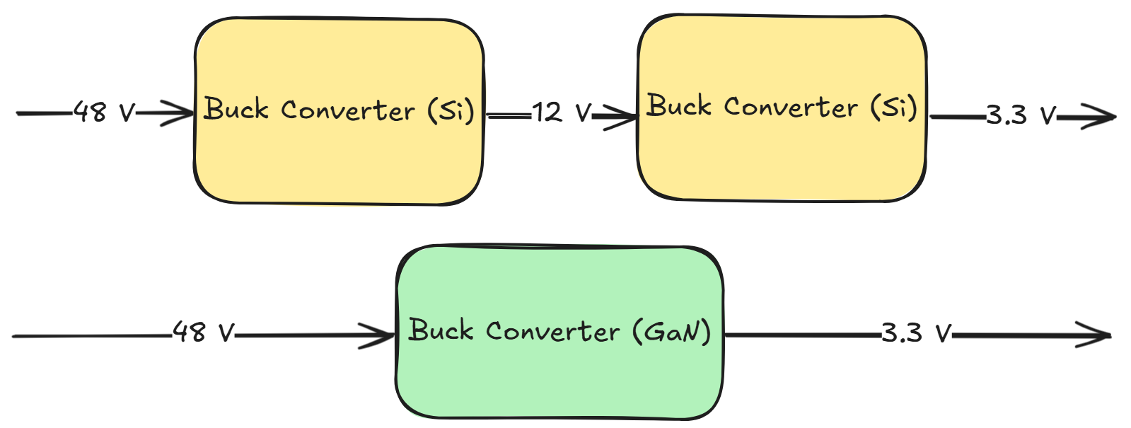
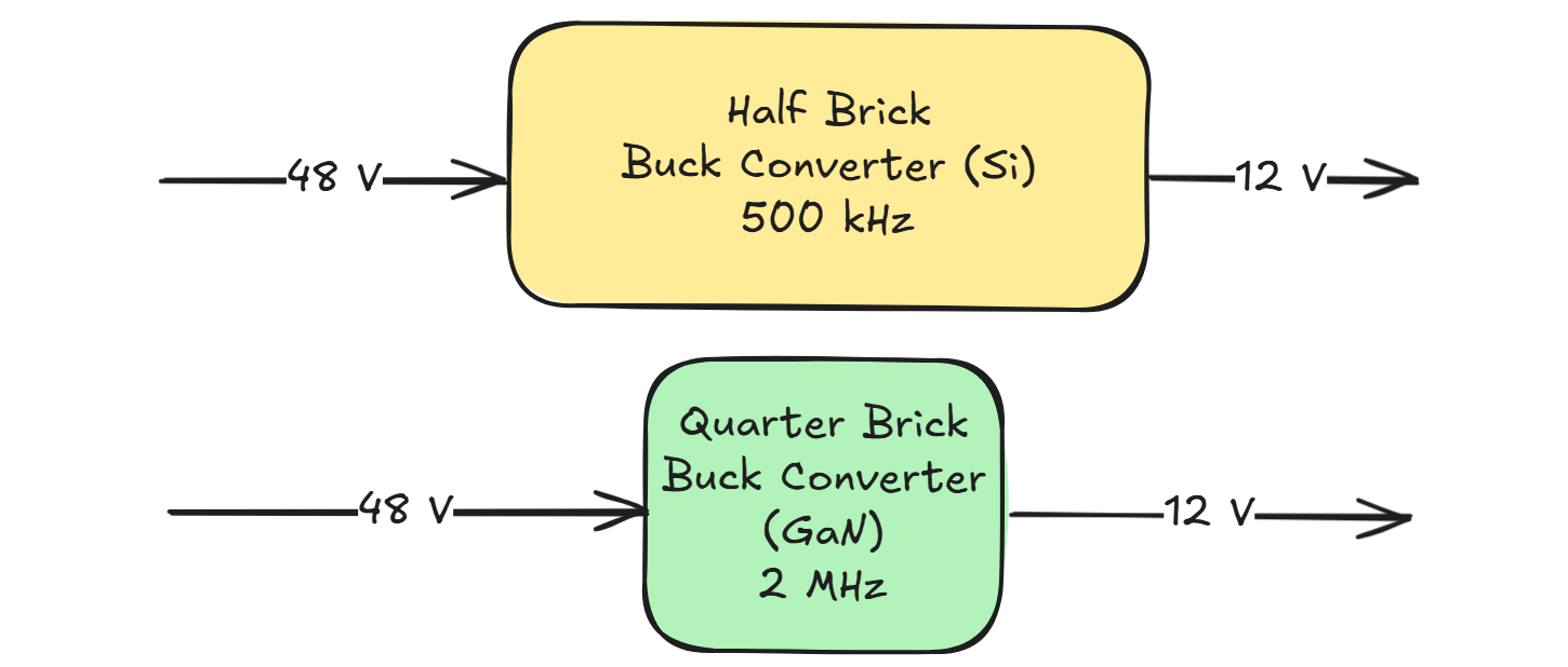
- The switching frequency can be increased by a factor of 2.5 to 3.
This allows, for example, a significant reduction in the form factor of a switching regulator.
The Rise of GaN and SiC in Power Electronics
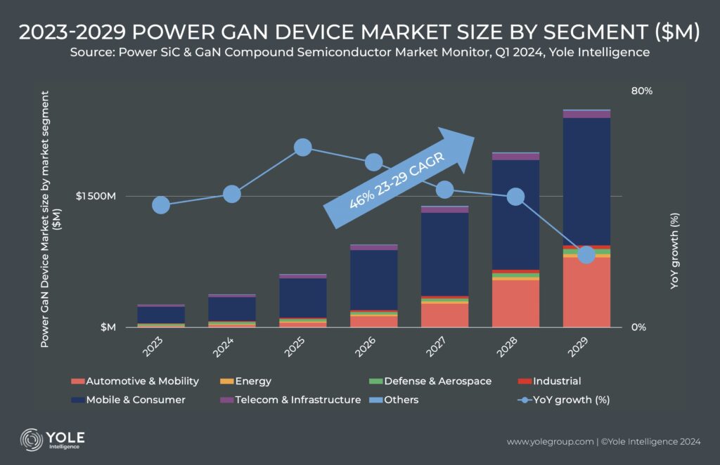
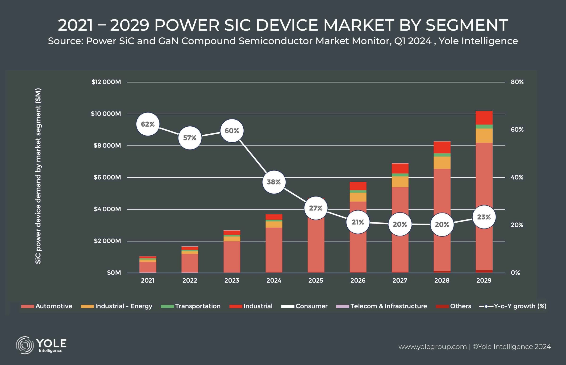
The manufacturing processes for power FETs based on wide band-gap materials such as GaN and SiC have been optimized, and high-volume production is established. As a result, GaN and SiC FETs are increasingly replacing conventional silicon power FETs and IGBTs. Market analyses confirm that this trend will continue, with the share of GaN and SiC devices steadily increasing over the coming years.
Further optimization of mature silicon FET technology requires significant financial investment for manufacturers. In contrast, GaN technology is still relatively young, offering substantial potential for both technical improvements and cost reductions.
"In the coming years, GaN technology is expected to evolve rapidly, paving the way for new architectural concepts and innovative design approaches…"
Sources
Figures
- *1: IMT AG
- *2: IMT AG
- *3: Analog Devices Webinar “Unleash the Benefits of GaN Technology with Advanced GaN Controllers and Gate Drivers” | Tag: Power Device Competitive Zone
- *4 Tag: Band gap diagram of metal, semiconductor and insulator
- *5: ST Microelectronics – Application note 5583 - E-mode GaN technology: tips for best driving
- *6 ST Microelectronics – Application note 5583 - E-mode GaN technology: tips for best driving | Tag: Basic structure of e-mode lateral GaN
- *7: https://www.analog.com/en/resources/evaluation-hardware-and-software/evaluation-boards-kits/eval-ltc7890.html | Tag: Analog Devices EVAL-LTC7890-AZ
- *8: https://www.yolegroup.com/strategy-insights/power-gan-harnessing-new-horizons/ |Tag: Power GaN Device Market
- *9: https://www.yolegroup.com/press-release/yg-press-news-despite-the-current-global-economic-challenges-the-growth-trajectory-of-silicon-carbide-sic-for-power-electronics-remains-intact/ | Tag: Power SiC Device Market
- *10: EPC – Application note AN002 - Fundamentals of Gallium Nitride Power Transistors | Tag: Theoretical resistance / voltage limits GaN, SiC and Si
Share


More Expert Blog articles
Discover IMT’s engineering expertise and innovative solutions in our Expert Blog. Gain valuable know-how from our experts and explore technology highlights.